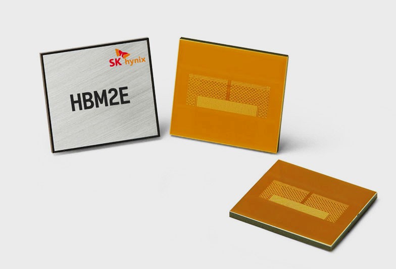
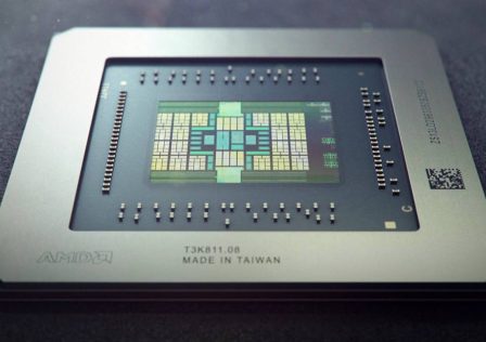
SK Hynix has just announced its latest in high-bandwidth DRAM technology rated at around 50% faster with doubly the density or capacity than traditional HBM2 memory. The new Hynix HBM2E memory will feature speeds up to 460GB/s which equates to 3.6Gbps per DRAM pin.
Memory density has also been increased twofold over HBM2 memory such as that found on the AMD Radeon VII. The new Hynix HBM2E memory will feature 16GB per chip. According to Hynix, this is possible through breakthroughts in TSV technology (Through Silicon Via) which relies on vertically stacking the chips thus increasing the density further.
“SK Hynix has established its technological leadership since its world’s first HBM release in 2013,” said Jun-Hyun Chun, Head of HBM Business Strategy. “SK Hynix will begin mass production in 2020, when the HBM2E market is expected to open up, and continue to strengthen its leadership in the premium DRAM market.”
While there is no telling when exactly we can expect to see compute GPUs featuring HBM2E memory, expect to see these new chips on both NVIDIA and AMD high end compute GPU products in the future.

